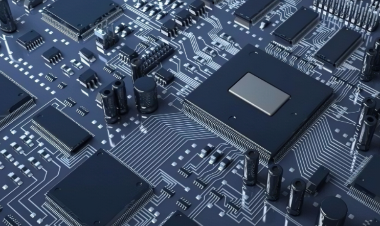
An integrated circuit or monolithic integrated circuit (also referred to as an IC, a chip, or a microchip) is a set of electronic circuits on one small flat piece (or "chip") of semiconductor material, usually silicon. Large numbers of miniaturized transistors and other electronic components are integrated together on the chip. This results in circuits that are orders of magnitude smaller, faster, and less expensive than those constructed of discrete components, allowing a large transistor count. The IC's mass production capability, reliability, and building-block approach to integrated circuit design has ensured the rapid adoption of standardized ICs in place of designs using discrete transistors. ICs are now used in virtually all electronic equipment and have revolutionized the world of electronics. Computers, mobile phones and other home appliances are now inextricable parts of the structure of modern societies, made possible by the small size and low cost of ICs such as modern computer processors and microcontrollers.
Very-large-scale integration was made practical by technological advancements in semiconductor device fabrication. Since their origins in the 1960s, the size, speed, and capacity of chips have progressed enormously, driven by technical advances that fit more and more transistors on chips of the same size – a modern chip may have many billions of transistors in an area the size of a human fingernail. These advances, roughly following Moore's law, make the computer chips of today possess millions of times the capacity and thousands of times the speed of the computer chips of the early 1970s.
ICs have three main advantages over discrete circuits: size, cost and performance. The size and cost is low because the chips, with all their components, are printed as a unit by photolithography rather than being constructed one transistor at a time. Furthermore, packaged ICs use much less material than discrete circuits. Performance is high because the IC's components switch quickly and consume comparatively little power because of their small size and proximity. The main disadvantage of ICs is the high initial cost of designing them and the enormous capital cost of factory construction. This high initial cost means ICs are only commercially viable when high production volumes are anticipated.

Terminology
An integrated circuit is defined as:
A circuit in which all or some of the circuit elements are inseparably associated and electrically interconnected so that it is considered to be indivisible for the purposes of construction and commerce.
In strict usage integrated circuit refers to the single-piece circuit construction originally known as a monolithic integrated circuit, built on a single piece of silicon.In general usage, circuits not meeting this strict definition are sometimes referred to as ICs, which are constructed using many different technologies, e.g. 3D IC, 2.5D IC, MCM, thin-film transistors, thick-film technologies, or hybrid integrated circuits. The choice of terminology frequently appears in discussions related to whether Moore's Law is obsolete.
A History
An early attempt at combining several components in one device (like modern ICs) was the Loewe 3NF vacuum tube from the 1920s. Unlike ICs, it was designed with the purpose of tax avoidance, as in Germany, radio receivers had a tax that was levied depending on how many tube holders a radio receiver had. It allowed radio receivers to have a single tube holder.
Early concepts of an integrated circuit go back to 1949, when German engineer Werner Jacobi (Siemens AG) filed a patent for an integrated-circuit-like semiconductor amplifying device showing five transistors on a common substrate in a three-stage amplifier arrangement. Jacobi disclosed small and cheap hearing aids as typical industrial applications of his patent. An immediate commercial use of his patent has not been reported.
Another early proponent of the concept was Geoffrey Dummer (1909–2002), a radar scientist working for the Royal Radar Establishment of the British Ministry of Defence. Dummer presented the idea to the public at the Symposium on Progress in Quality Electronic Components in Washington, D.C. on 7 May 1952.He gave many symposia publicly to propagate his ideas and unsuccessfully attempted to build such a circuit in 1956. Between 1953 and 1957, Sidney Darlington and Yasuo Tarui (Electrotechnical Laboratory) proposed similar chip designs where several transistors could share a common active area, but there was no electrical isolation to separate them from each other.
The monolithic integrated circuit chip was enabled by the inventions of the planar process by Jean Hoerni and p–n junction isolation by Kurt Lehovec. Hoerni's invention was built on Mohamed M. Atalla's work on surface passivation, as well as Fuller and Ditzenberger's work on the diffusion of boron and phosphorus impurities into silicon, Carl Frosch and Lincoln Derick's work on surface protection, and Chih-Tang Sah's work on diffusion masking by the oxide.
 繁體(台灣)
 简体中文
简体中文 USA(English)
 Vietnam